Jul 16, 2025
Comparing SMD, MIP, and COB: LED Display Packaging Technologies
There are several packaging technologies used in LED display. Among them, this post focuses on SMD (Surface-Mounted Device), MIP (Micro in Package), and COB (Chip on Board).
SMD Technology: Wire Bonding and GOB
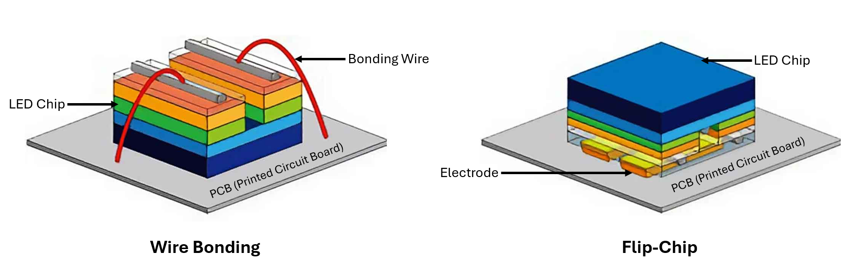
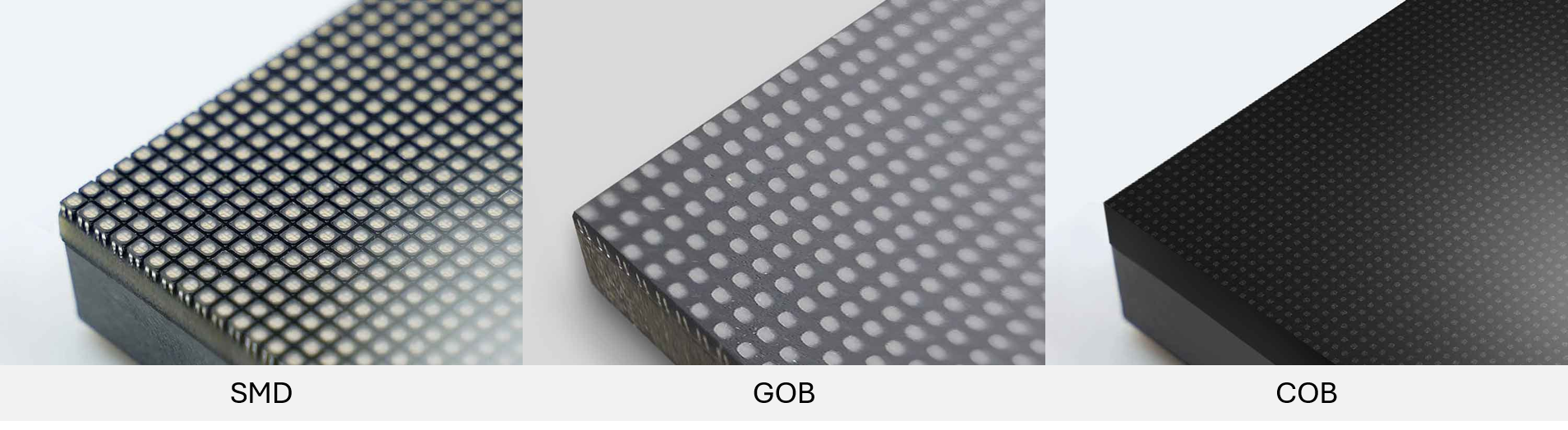
SMD technology can be classified into two categories: wire bonding and flip-chip. Typically, SMD refers to the wire bonding type, which is the most common and traditional LED display method. In SMD technology, individual RGB (red, green, blue) LED chips are first packaged and then surface-mounted onto a printed circuit board (PCB) with wires connecting the LED to the PCB. SMD is suitable for both indoor and outdoor displays with larger pixel pitches (greater than P2.5), such as large advertising screens and general-purpose indoor displays.
If a protective transparent glue is applied over the surface of SMD LED module, it is referred to as GOB (Glue on Board). This glue layer improves durability by protecting against dust, moisture, and physical impact. GOB is commonly used in displays with touch options.
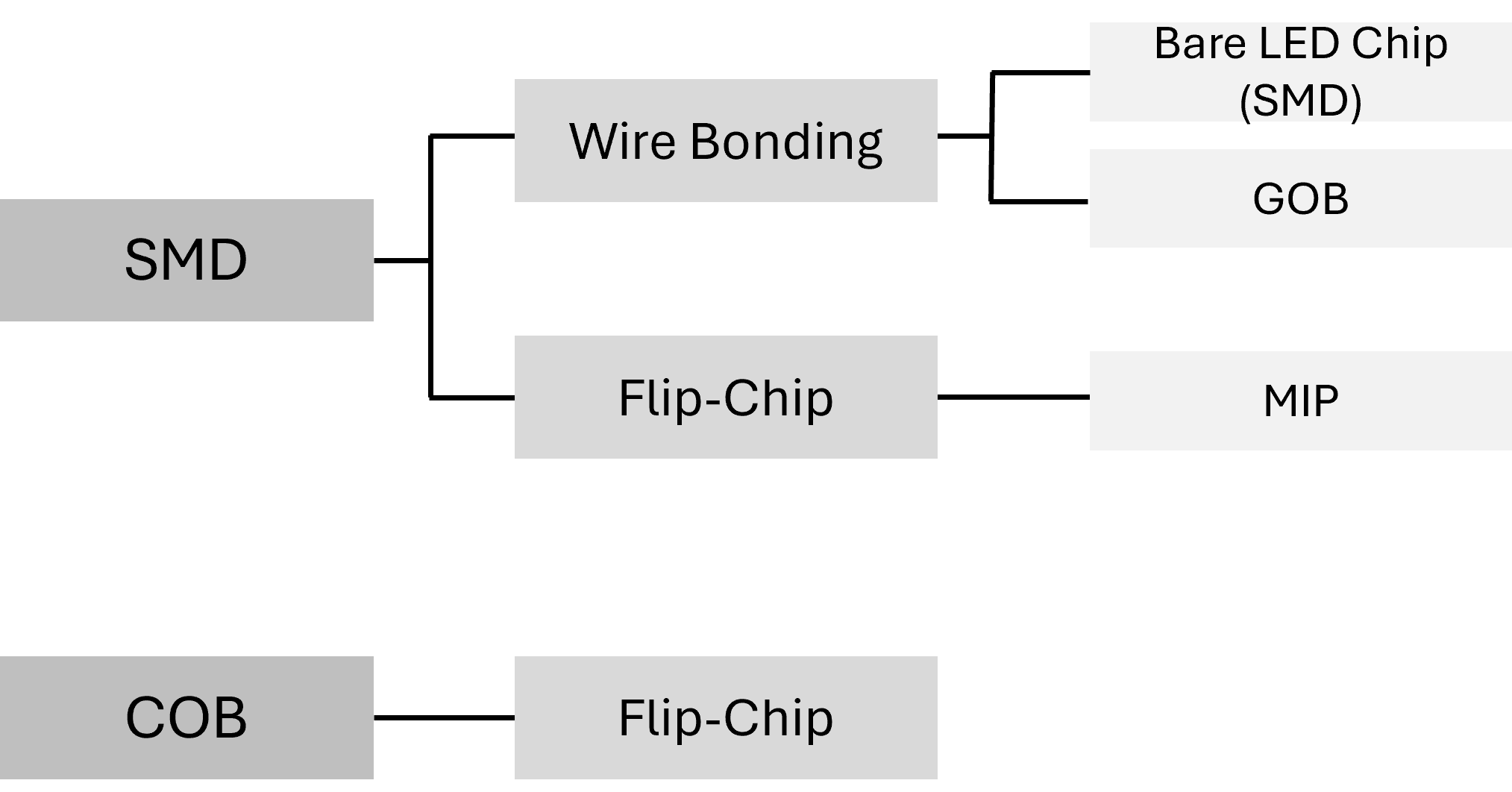
SMD Technology: Flip-Chip and MIP
Flip-chip technology involves mounting LED chips upside down so they can be directly connected to the PCB without wires. In SMD technology, MIP uses flip-chip technology. MIP involves densely integrating Micro LED chips into ultra-compact packages, which are then surface-mounted onto the PCB. While conceptually similar to SMD, MIP differs in that it uses flip chips and significantly smaller LED chips. MIP is optimized for Micro LED applications and is ideal for premium displays requiring high brightness, high contrast, and excellent color uniformity, such as AR/VR devices and wearables. Its pixel pitch is between P0.9 and P2.5.
Flip-chip technology is generally more efficient than wire bonding. Without wire connections, the structure is simpler and more durable, with no risk of wire damage. Additionally, because LED chips are directly bonded to the PCB, the heat dissipation path is shorter, enabling better thermal management and more stable performance. No wire also allows the chips to be placed closer to the PCB, resulting in smaller pixel pitches for high-resolution displays.
COB Technology
COB also uses flip-chip technology but differs significantly from MIP. In COB, LED chips are directly mounted onto the PCB without individual packaging, whereas SMD, GOB, and MIP all involve packaged chips. As with MIP, the flip chip configuration in COB allows for high brightness, excellent energy efficiency, and enhanced durability. COB is widely used for indoor applications that require high resolution, short viewing distances, and small pixel pitches (typically between P0.6 and P1.8), such as conference rooms and broadcast studios. Due to its improved durability and superior thermal performance, COB also significantly reduces the need for pixel repair.
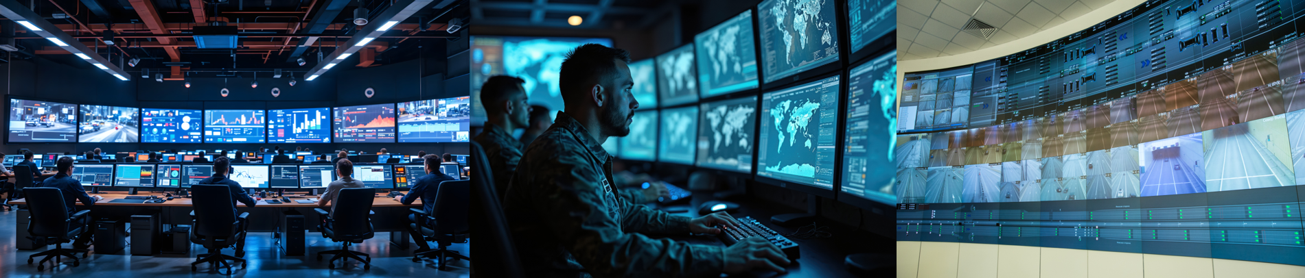
As mentioned above, MIP and COB technologies are commonly used in premium TVs, conference rooms, and broadcast studios. Due to their support for fine pixel pitches and high resolution, they are also well-suited for command-and-control rooms, where such capabilities are essential. In the United States, products used in command-and-control room or military applications must comply with the Trade Agreement Act (TAA). To meet these requirements, BSI has established a production facility in South Korea, ensuring that all products are TAA-compliant. Both COB and MIP manufacturing will take place in South Korea. As a result, our LED display solutions offer a reliable and compliant choice for customers seeking TAA-certified products.